Solid State Musik PB1
- Introduction
- For Your Safety
- Settings
- Tests
- Improvements
- Contemporary Witnesses
- Internal Links
- External Links
- Technical Manuals
- References
Introduction

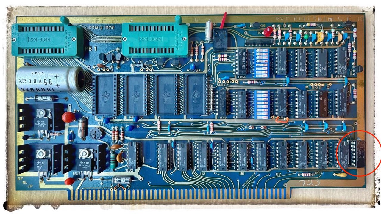
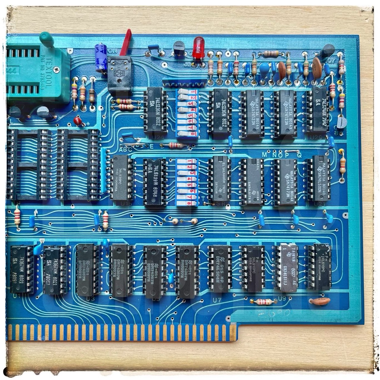
The special thing about the boards of Solid State Music is the blue color of the PCB ("We used to be Solid State Music. We still make the blue boards."). My 2nd board (#723) is also characterized by the fact that the tracks look gold-plated, see next.
- Engraving: PROPERTY OF DVC ELECTRONICS CLUB -
Board #723 is a modified version, maybe done by DVC Electronics Club.. I don't have the knowledge to evaluate this modification. My tests have shown that the 2708 can be read and the 2716 can be read and programmed. As I have two boards, this is set to 2716 and the other to 2708. Therefore the programming voltage is set to 25V (2716).
The DVC abbreviation could be interpreted as Diablo Valley College (Pleasant Hill, CA 94523, USA).
My Rating
In addition to this card, I also have the comparable one from Cromemco, the 8K Bytesaver. In my experience so far, the Cromemcon 8K Bytesaver is more reliable when it comes to providing the programming voltage (25V).
As far as reading and addressing are concerned, I can report that this works perfectly with the SSM-PB1.
For Your Safety
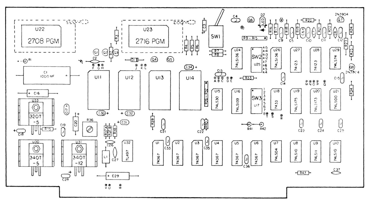
Program Power Switch
The red switch (SW1) in the middle top should always be set to OFF to prevent uncontrolled writing of an EPROM.
Settings
I am currently using the SSM-PB1 in my N* Horizon with the Vector 4.0C monitor. Therefore the memory areas B and E are a no-go. This leaves only C000-DFFF. Thus only a 48K CP/M can be used.
Selection of EPROM Type
2708
---------
A-E (A10)
B-D (A11)
F-H (-5V)
J-K (+12V)

2716
---------
B-E (A11)
C-D (A12)
F-G (+5V)
J-L (A10)
Reading
⇓ SW3: 0 0-1-0-0-1-0 0 (this is 2708 & C000h)
⇒ right pressed is ON or 1
⇐ left pressed is OFF or 0
2708:    set SW3-1 to OFF
-------------------------------
SW3       2  3   4   5   6   7
-------------------------------
8000     OFF ON  ON OFF OFF OFF
A000     OFF ON OFF  ON OFF OFF
C000     OFF ON OFF OFF  ON OFF   <- my address for the N*
E000     OFF ON OFF OFF OFF  ON
9000     ON OFF  ON OFF OFF OFF
B000     ON OFF OFF  ON OFF OFF
D000     ON OFF OFF OFF  ON OFF
F000     ON OFF OFF OFF OFF  ON

2716:    set SW3-1 to ON
--------------------------------
SW3       2   3   4   5   6   7
--------------------------------
8000     OFF OFF  ON OFF OFF OFF
A000     OFF OFF OFF  ON OFF OFF
C000     OFF OFF OFF OFF  ON OFF  <- my address for the N*
E000     OFF OFF OFF OFF OFF  ON

(SW3-8 is not used)
Programming
⇑ SW2: 1-1-0-1 0-0-0-1 (this is D000h & port 10h)
⇒ right pressed is ON or 1
⇐ left pressed is OFF or 0
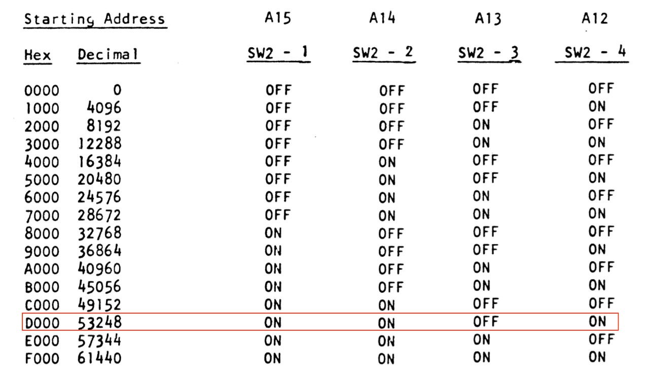
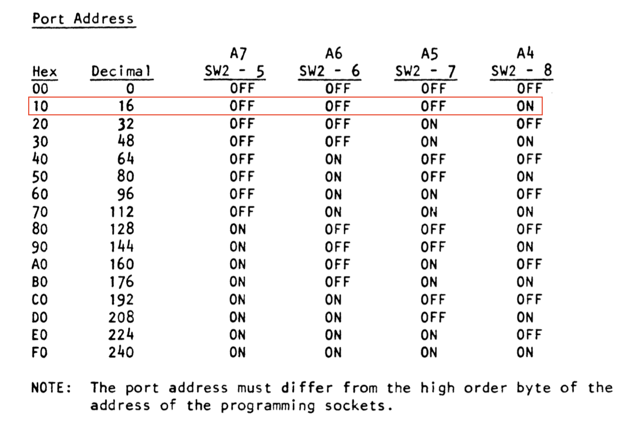
I can't say yet (1st Nov 2023) if the port address of 10h is correct for my N* Horizon; need to research further. But the read address with C000h is correct and the programming address with D000h should be as well.
Tests
Circuit Board Check
To avoid short circuits, the following check is always recommended in the old S-100 board building instructions. Actually, it is mandatory.
Check every unkown board to ensure that the +8, +16, -16 volt buses are not shorted to one another or to ground (GND). Using an ohmmeter (multimeter), make the following measurements. You should measure no continuity (no beep) in any of these measurements.
Negative voltages (7905) are of course only needed by a few S-100 cards but these are the most dangerous ones.
These simple tests take a maximum of five minutes, but can save you several hours of work!
Reading
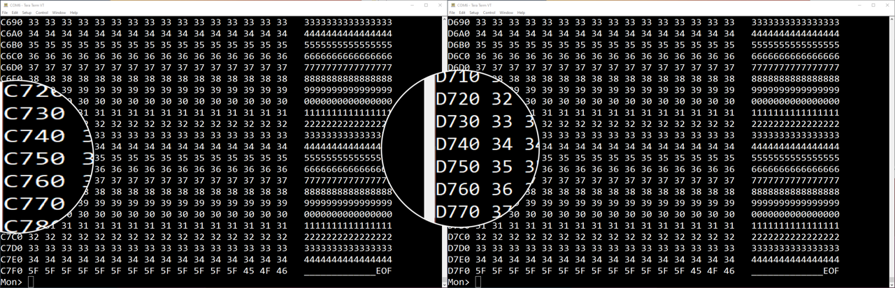
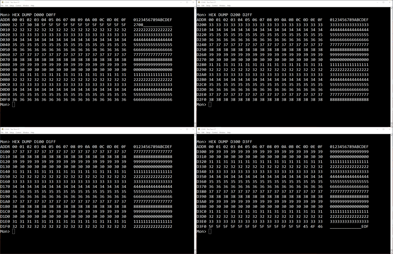
I have tested the PROM reading with 2708 and 2716 EPROMs. For this I have written the EPROM in question with easy to read test data. An error can be recognized so visually immediately.
I have read from both C000 and D000 - my two address ranges. The result was correct.
The only disadvantage of this board is that you have to change the jumper connections when changing from 2708 to 2716 because of the different voltages. But this is not a problem for me, because I have two boards.
Programming
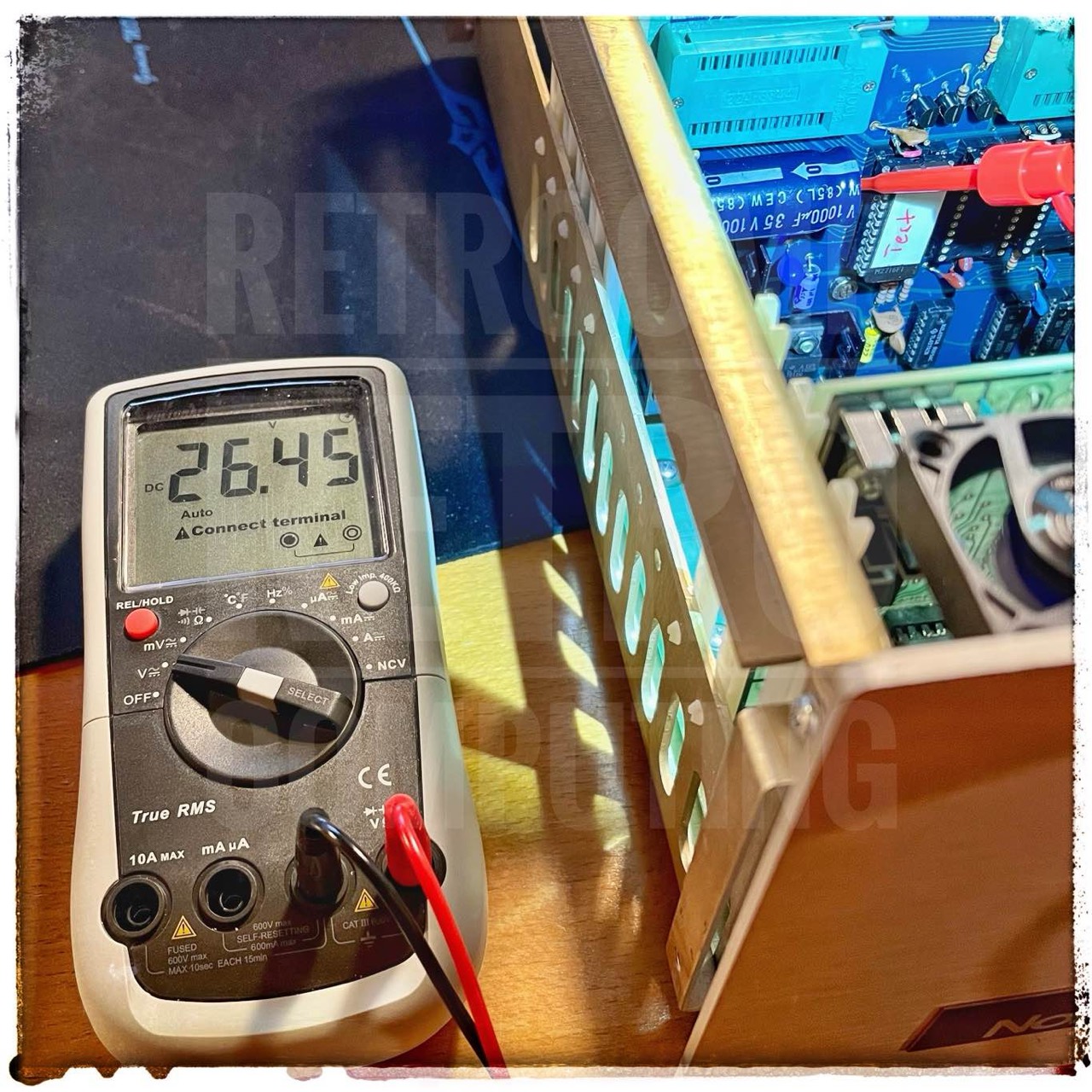
Before programming, be sure to check the programming voltage. And this is where the manual is inaccurate. Why? The manual describes on page 2-1 that the programming voltage should be set to +26.5V using the trimpot (R36). This is correct for a 2708 EPROM (min=25V, max=27V), but not for the 2716 EPROM (min=24V, max=26V).
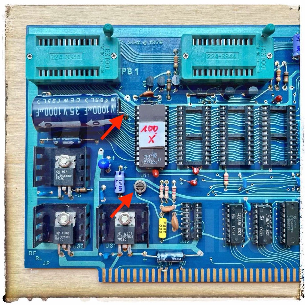
First, I (pre) adjusted the trimpot to 5-10 kΩ. For this I removed U32; the IC must of course be put back in! Measure at pin 1 and 6.
For a first test run I used the original program from SSM. As data source I simply used one of my test EPROMs at C000h. As return address I use E000h, this is the start address of my monitor (Vector 4.0C) in the N*.
2716
The programming time with the following code should be about 100 seconds.
;A SIMPLE ROUTINE FOR PROGRAMMING 2716'S
;COPYRIGHT BY SOLID STATE MUSIC, 1978

;REGISTER USAGE:
;REG.A....PASS DATA FROM MEMORY TO THE PROGRAMMER
;REG.B....REPEATED PROGRAMMING CYLES
;REG.DE...PROM CARD ADDRESS
;REG.HL...DATA ADDRESS TO BE COPIED

LOC     EQU     100H

;SET THESE EQUATES TO MATCH YOUR CONFIGURATION
PROM    EQU     0D000H  ;PROGRAMMING SOCKET
RAM     EQU     0C000H  ;DATA TO BE COPIED
CPORT   EQU     10H     ;CONTROLPORT FOR PB1
MONIT   EQU     0E000H  ;EXIT ADDRESS SET BY USER, VECTOR 4.0C

        ORG     LOC
;START OF PROGRAM
;INITIALIZE BOARD
PROG0:  MVI     A,02    ;02=2716
        OUT     CPORT   ;RESET BOARD

;SET UP PARAMETERS
;NUMBER OF PROGRAMING CYCLES
        MVI     B,01    ;ONE CYCL FOR 2716

;NUMBER OF BYTES =256(C+1)
;                =256x8=2048 or 2KB
        MVI     C,07    ;07=2716

;SET UP ADDRESS FOR TRANSFER
PROG1:  LXI     D,PROM
        LXI     H,RAM

;PROGRAM THE EPROM
PROG2:  MOV     A,M
        STAX    D
        INX     D
        INX     H
        MOV     A,D
        ANA     C
        ORA     E
        JNZ     PROG2
        DCR     B
        JNZ     PROG1
        DCX     D
        LDAX    D       ;RESET PB1
        JMP     MONIT   ;BACK TO MONITOR

;END OF PROGRAM
	END
And this is the result.
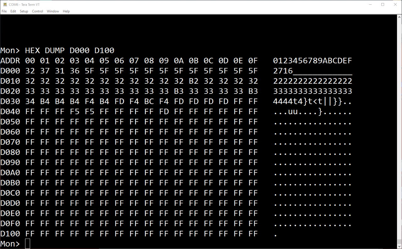
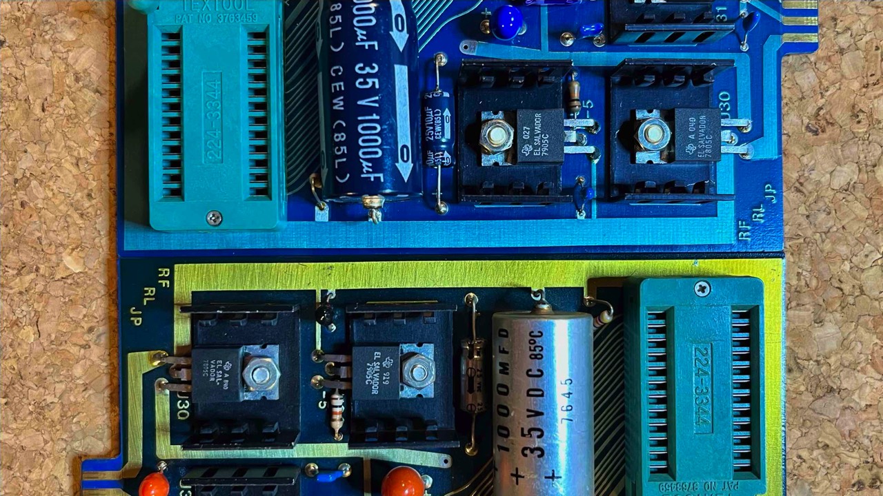
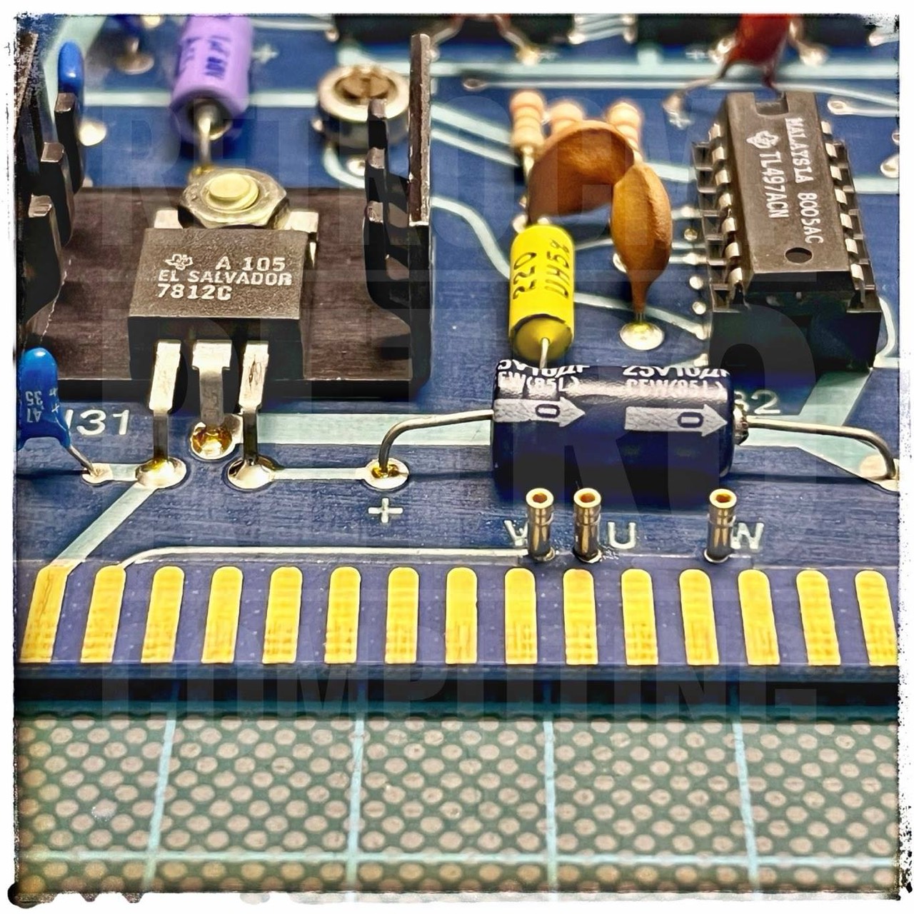
I found out very quickly that the programming voltage drops to 18V very quickly, so the first bytes are fine. But I do not know why the voltage drops. Maybe the big capacitor (35V, 1000µF) is too old.
Checking this capacitor showed: the capacitance is 1,120 µF and the ESR is 0.2 Ω. According to the various tables on the Internet, the ESR in this case should be <0.11 Ω. But these are only reference values. The capacitor would be defective if it would be above 1 Ω, but 0.2 instead of 0.1. That can not be the error.
Error source no. 1: I have leafed through the manual and there the U32 TL497ACN (DC-DC converter) is mentioned as a possible error source. Since I have a second PB1 board, I could quickly swap and see that it works better. I would say 95% were programmed correctly, the rest has errors.
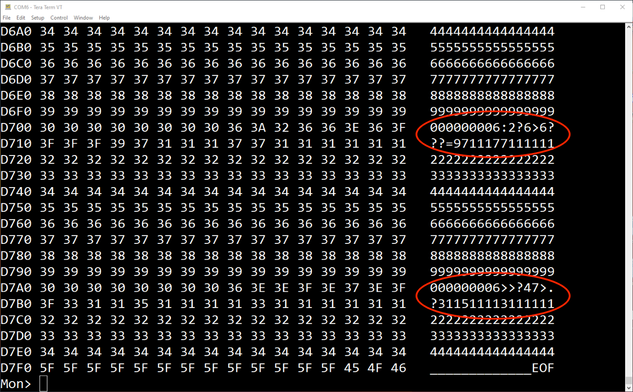
Update 11/05/2023: Using my second PB1, I finally realized that there can be three problem points with the power supply. Trim potentiometer, DC-DC converter and the capacitor C1; check all oh them. The EPROM may also be defective and/or draws too much voltage.
2708
I use 100 (64H) programming loops or cyles. More about the actual programming process can be found at EPROM 2708. The programming time with the following code should be ab 160 seconds.
;A SIMPLE ROUTINE FOR PROGRAMMING 2708'S
;COPYRIGHT BY SOLID STATE MUSIC, 1978

;REGISTER USAGE:
;REG.A....PASS DATA FROM MEMORY TO THE PROGRAMMER
;REG.B....REPEATED PROGRAMMING CYLES
;REG.DE...PROM CARD ADDRESS
;REG.HL...DATA ADDRESS TO BE COPIED

LOC     EQU     100H

;SET THESE EQUATES TO MATCH YOUR CONFIGURATION
PROM    EQU     0D000H  ;PROGRAMMING SOCKET
RAM     EQU     0C000H  ;DATA TO BE COPIED
CPORT   EQU     10H     ;CONTROLPORT FOR PB1
MONIT   EQU     0E000H  ;EXIT ADDRESS SET BY USER, VECTOR 4.0C

        ORG     LOC
;START OF PROGRAM
;INITIALIZE BOARD
PROG0:  MVI     A,01    ;01=2708
        OUT     CPORT   ;RESET BOARD

;SET UP PARAMETERS
;NUMBER OF PROGRAMING CYCLES
        MVI     B,64H   ;50-255 FOR 2708, 64H=100D

;NUMBER OF BYTES =256(C+1)
;                =256x4=1024 or 1KB
        MVI     C,03    ;03=2708

;SET UP ADDRESS FOR TRANSFER
PROG1:  LXI     D,PROM
        LXI     H,RAM

;PROGRAM THE EPROM
PROG2:  MOV     A,M
        STAX    D
        INX     D
        INX     H
        MOV     A,D
        ANA     C
        ORA     E
        JNZ     PROG2
        DCR     B
        JNZ     PROG1
        DCX     D
        LDAX    D       ;RESET PB1
        JMP     MONIT   ;BACK TO MONITOR

;END OF PROGRAM
	END
And this is the result.
And now comes the 1 million dollar question. Why can I program 2708 EPROMs with the same PB1 but not 2716? I have only changed the settings from 2716 to 2708 and nothing else.
Software for Programming
More about the actual programming process can be found at EPROM 2708.
Improvements
I put a second one on each of the existing sockets, since the EPROMs are easier to remove that way. Some capacitors are directly placed at the socket.
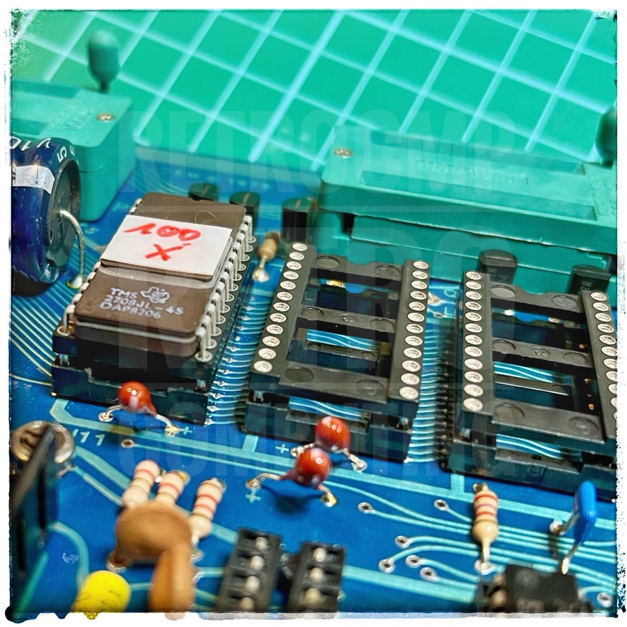
Furthermore I replaced all hard soldered jumper connections A to V with pin receptacles by Mill-Max (0240-0-15-01-30-27-04-0).
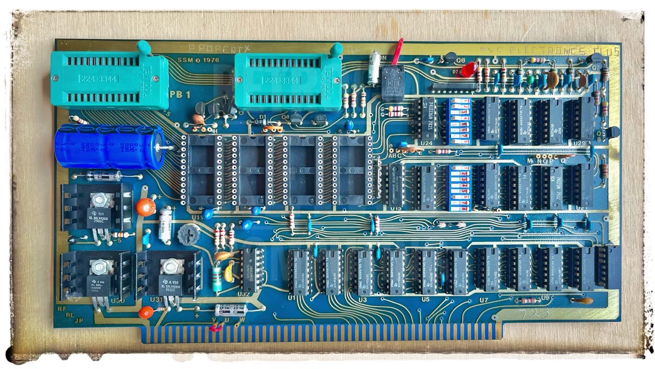
new: cap C1, U32 DC-DC, four additional sockets
Contemporary Witnesses
Robert Roeder:
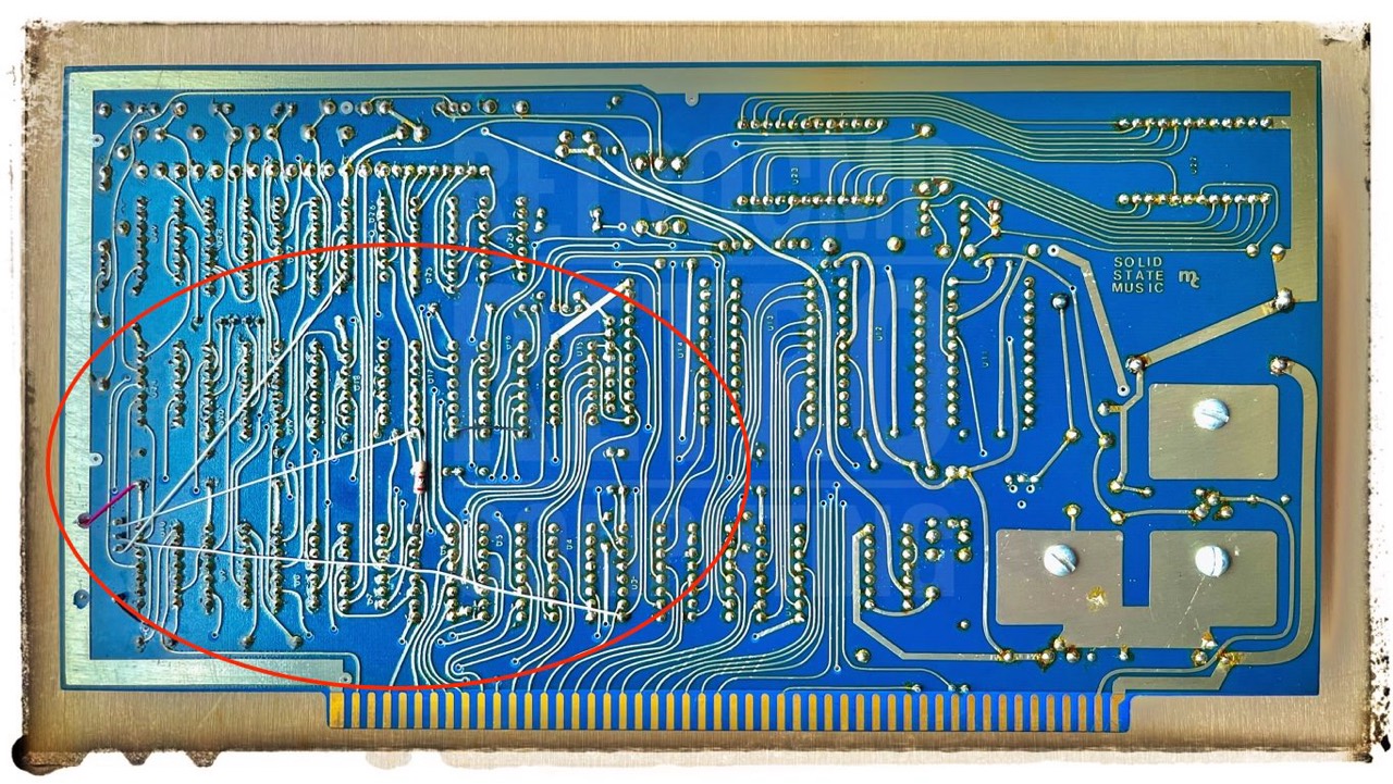
I always look back on boards like this with the fluid trace routing and cringe
Joe Travis:
Really? I tend to admire and appreciate the artwork of a well hand laid out board.
Robert Roeder:
The problem inconsistent spacing, sometime too close for manufacturing in that era. 8 mil traces between dip pads. The standard DIP pattern was one .06x.06 square pad, and the rest .06 round pads. Bishop Graphic later produced (1976) dip patterns where the round pins were cut. .06 long and .04 wide. This also was the same era that pinned Mylar was being used, obsoleting red/blue markup with a common pad master. This allowed a .08 trace with .01 clearance on either side. Any bend in the trace could cut trace clearance too close. Look at the memory section and see the 45 deg cutwork. Doug Douglass from Douglas Electronics shifted the dip pattern 5 degs so he could run a straight trace thru. Also remember in this era was before computerized drilling and all was hand drilled. The holes needed to be bigger than the final size before plating and screening the resist to the board. Later 1978 and above a photo resist was applied to the pcb and exposed to the master film. [1]
Internal Links
External Links
- S100 Computers: Solid State Musik PB1 - EPROM Programmer Board
Technical Manuals
- PB1 2708/2716 Programmer & 4K/8K EPROM Board Instruction Manual, 1979?
- PB1 2708/2716 Programmer & 4K/8K EPROM Board Instruction Manual, 1983